On the circuit board of the Wavedrum there are solder holes to accomodate three large connectors. Since they are so easily accessible and thus very inviting to anyone interested in modifying the instrument, I decided to trace each of the pins to its destination.
The three connectors are named CN10, CN11, and CN12, respectively. CN10 is found on the bottom right, CN11 on the bottom left, and CN12 close to the left edge below the micro SD card reader.

Most of the ten pins of CN10 are outputs. The first three pins
carry clock signals used by the analogue to digital and digital
to analogue converters on the top-side of the board. Pin four
gives access to the PDN (power down) signal which is used to
disable the converters. The next three pins are connected over
the resistors R85, R84, and R83 to the DSP's pins 145, 144, and
143 (respectively); according to the DSP's datasheet these pins are DAI_P8 (SFSI), DAI_P10
(SD2B), and DAI_P11 (SD3A), and are thus part of the
Digital Audio Interface (DAI). The remaining three pins on CN10
expose the supply voltage, ground, and an alternative positive
voltage (the same as on the plus pole of the silver capacitors
near the right edge of the board). These are the signals left to
right:
| direction | description | |
|---|---|---|
| 1 | output | Master clock |
| 2 | output | Audio serial clock |
| 3 | output | Left/right clock |
| 4 | output | PDN (power down) |
| 5 | input? | DAI_P8 / SFSI |
| 6 | input? | DAI_P10 / SD2B |
| 7 | input? | DAI_P11 / SD3A |
| 8 | output | V_A, or V_DD |
| 9 | output | GND |
| 10 | output | alternative positive voltage |
What is this all good for? Well, since all these clocks and
voltages are exported it becomes relatively easy to connect an
external digital to analogue converter (when DAI_P8,
DAI_P10, and DAI_P11 are used as outputs), or
an external analogue to digital converter (if the DSP pins are
used as inputs instead). nAs there are protective resistors
between the DSP pins and the connector pins 5–7 I assume that
they are supposed to be used as inputs.
Moving on to the left bottom edge of the board we see a 14-pin connector with the name CN11. This connector gives access to the JTAG interface on the DSP, which allows system debugging. Unfortunately, I don't own a JTAG dongle and the free JTAG debugger OpenOCD does not support the SHARC core, so I haven't been able to experiment with the debugging interface. I'm not sure whether it is possible to use debugging feature without hardware/software provided by Analog Devices. Using JTAG it should be possible to overwrite the flash memory and replace the firmware. This is the most promising method to upgrade (or downgrade) a Wavedrum.
The pins on the bottom row are all connected to ground, so the following table only lists the signal names of the upper row of the connector in order from left to right:
| Signal | Full name | |
|---|---|---|
| 1 | | Emulation status |
| 2 | | Ground |
| 3 | | Test mode select |
| 4 | | Test clock |
| 5 | | Test reset |
| 6 | | Test data input |
| 7 | | Test data output |
CN12 exposes the DSP's two-wire interface, a serial interface compatible with the proprietary I^2C interface. This allows us to connect a number of external serial devices to the serial bus. As firmware support is required to communicate with the devices on the serial bus I don't see how this could be used without a custom firmware.
The following table lists the signals from top to bottom:
| Signal | Full name | |
|---|---|---|
| 1 | | Positive voltage |
| 2 | | Two-wire interface data |
| 3 | | Two-wire interface clock |
| 4 | | Ground |
What led me to tracing the routes of the connectors was my
curiosity about the boot mode. According to the DSP's datasheet,
there are four possible boot modes to select from by playing with
the states of the pins BOOT_CFG1-0 (one of these boot
modes is “no boot”). Tracing these two pins from the DSP it
becomes clear that the third boot mode “EPROM/FLASH boot” is
hardwired (BOOT_CFG1-0 = 10). The other two usable
boot modes are SPI master and slave boots.
| BOOT_CFG1-0 | Booting mode |
|---|---|
| 00 | SPI Slave Boot |
| 01 | SPI Master Boot |
| 10 | EPROM/Flash Boot |
| 11 | No boot |
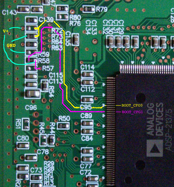
As can be seen on the photo, the Wavedrum engineers were kind
enough to leave solder pads connected to boot configuration pins
on the board, allowing us to rewire them as we see fit. To set
BOOT_CFG0 the pads for R72 have to be
bridged; likewise, to clear BOOT_CFG1 only the two pads
of R59 have to be bridged.
Comments? Then send me an email! Interesting comments may be published here.